Modern computers contain billions of transistors that work together to create our digital world. However, most people don’t understand how these sophisticated machines actually work at the fundamental level. To truly grasp computer architecture and digital logic, I built a complete 8-bit computer entirely from basic logic gates and discrete components.
This project required designing a custom Instruction Set Architecture (ISA). Additionally, I implemented a microcoded control unit. Furthermore, I constructed every component from 74-series TTL logic chips. As a result, I created a fully functional computer that executes programs, performs calculations, and demonstrates the fundamental principles underlying all modern computing systems.
Architecture Overview:
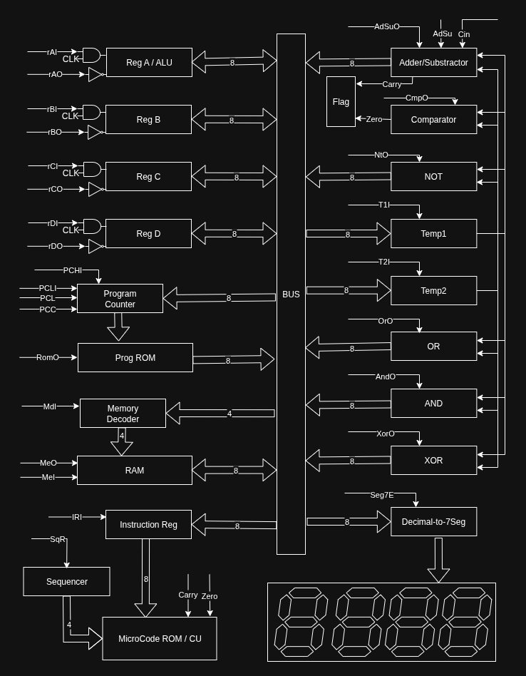
I built the computer around a traditional bus-based architecture. Specifically, separate functional units connect via an 8-bit data bus. The system includes four general-purpose registers (A, B, C, D). Moreover, it features a custom arithmetic logic unit (ALU), 16 bytes of RAM, and a sophisticated program counter. A 7-segment display module is included for visual output, driven by a custom circuit interfaced with the data bus. Finally, a microcoded control unit orchestrates all operations.
The instruction set uses a 15-bit format optimized for this architecture. It supports arithmetic operations (ADD, SUB) and logical operations (AND, OR, XOR, NOT). Additionally, it includes memory operations (LDI, LDM, SAV) and control flow instructions (JMP, JMZ, JNZ, JMC). Furthermore, I implemented flag-based conditional operations using Zero and Carry flags. This enables sophisticated program logic, including loops and conditional execution.
Hardware Implementation:
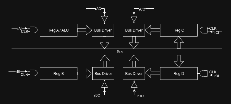
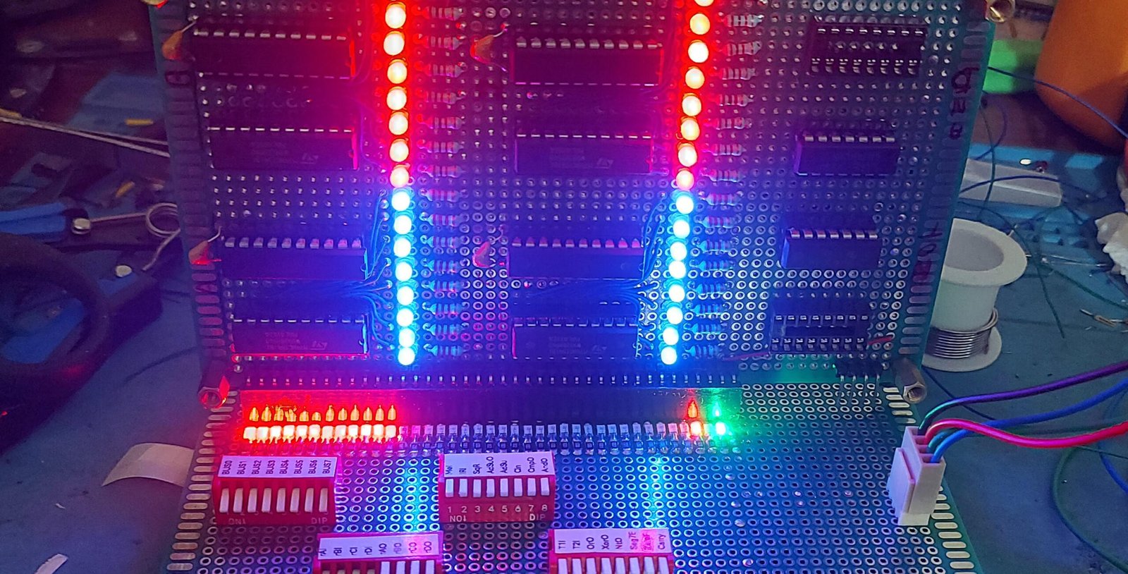
I constructed every component using discrete 74-series TTL logic chips. These are the same chips that powered computers in the 1970s and 80s. Specifically, I implemented the general-purpose registers with 74LS574 8-bit register chips. Meanwhile, the ALU uses 74LSxx adders and 74LS86 XOR gates to perform arithmetic and logical operations. Additionally, the memory system utilizes 74LS189 RAM chips, providing 16 bytes of storage.
I built the entire system on general-purpose breadboards and perfboards rather than custom PCBs. Consequently, every connection remains visible and debuggable. Furthermore, LED indicators throughout the system provide real-time visualization of data flow, register contents, and control signals. This approach offers complete transparency into every aspect of the computer’s operation. Although it’s more complex than using modern integrated solutions, it provides valuable insights.
The modular design separates major functional units onto individual boards. These include registers, ALU, memory, and control units. As a result, this facilitates debugging and allows systematic testing of each component. When issues arise during development, I can isolate problems to specific modules. Therefore, I can resolve them independently.
Control System:
Rather than implementing hardwired control logic, I used a sophisticated microcode approach. Each instruction breaks down into a sequence of micro-operations stored in ROM. For example, when executing an ADD instruction, the microcode sequence first enables register A onto the bus. Then it routes register B to the ALU. Next, it performs the addition operation. Subsequently, it stores the result back to register A. Finally, it updates the processor flags.
This microcode system provides exceptional flexibility. Specifically, I can modify the instruction set simply by reprogramming the control ROMs. Furthermore, I generate the microcode using Python scripts that define each instruction’s behavior. These scripts handle control signals and timing, then automatically generate the binary data for the ROM chips.
Software Development Tools:
I developed a complete software toolchain to program the computer. The custom assembler translates human-readable assembly language into binary machine code. Moreover, it’s compatible with the 15-bit instruction format. It supports mnemonic instructions and symbolic labels for program navigation. Additionally, it includes comprehensive error checking to catch programming mistakes during development.
The assembler outputs binary files that load directly into the computer’s memory. Programs can include arithmetic calculations and logical operations. Furthermore, they support control flow with loops and conditionals. Additionally, programs can handle memory manipulation and output display routines for the 7-segment display system.
Microcode Generation Framework:
The microcode generation tools represent some of the most sophisticated software in the project. I wrote these tools in Python. They define every instruction’s precise behavior in terms of control signals, bus operations, and timing requirements. Furthermore, adding new instructions requires only updating the Python definitions. Then I regenerate the microcode ROMs.
I also developed an Arduino-based microcode flasher to program the control ROMs. This provides a simple interface for uploading new microcode versions during development and testing.
Practical Applications:
Despite its simplicity compared to modern computers, this system can execute real programs. These include mathematical calculations, algorithm implementations, and control flow demonstrations. Additionally, it runs simple interactive programs. One demonstration program generates Fibonacci sequences. It computes and displays each number on the 7-segment display. Meanwhile, every computational step remains visible through the LED indicators.
The 16-byte memory limitation forces extremely efficient programming practices. Consequently, it requires creative solutions to implement useful functionality within severe constraints. Although this limitation is restrictive, it provides valuable insights into memory management and code optimization techniques.
Technical Specifications:
- Architecture: 8-bit bus-based design with microcoded control
- Instruction Format: 15-bit instructions with custom encoding
- Registers: Four general-purpose 8-bit registers (A, B, C, D)
- Memory: 16 bytes using 74LS189 RAM chips
- ALU Operations: ADD, SUB, AND, OR, XOR, NOT, CMP
- Control Flow: Conditional jumps based on Zero and Carry flags
- Display: 7-segment decimal output with custom driver circuit
- Clock: Manual stepping with LED status indicators
- Technology: 74-series TTL logic, no microcontrollers or programmable devices
Project Repository:
You can find the complete project documentation, source code, and schematics at: https://github.com/arghyabi/Computer8Bit
The repository includes the custom assembler and microcode generation tools. Additionally, it contains Arduino flasher firmware and comprehensive technical documentation. Furthermore, it provides example programs demonstrating the computer’s capabilities.
Leave a Reply